


焊球栅网阵列的热建模
日期:2012-06-20
Thermal Modeling of Ball Grid Arrays |
||||||||||||||||||||||||||||||||||||||||||||||||||||||||||||||||||||||||||||||||||||||||||||||||||||||||||||||
|
Dr. Pavel Valenta
Thermal performance of ball grid array packages for applications in telecommunications was investigated by FLOTHERM simulations. First some guidelines for the thermal modeling were established by comparison of simulation results and junction temperature measurement done on a standard Plastic BGA. Then the guidelines were applied to the modeling of the thermally enhanced package SuperBGA mounted on multilayer boards with different copper layer thicknesses. The results were analyzed to get the package thermal resistance for different applications and to understand the distribution of the heat fluxes to different flow paths. Due to the pressure of cost reduction and miniaturization in transmission and switching systems, the currently used Ceramic Pin Grid Arrays (CPGA) and Ceramic Quad Flat Packages (CQFP) have to be replaced by cheaper solutions. Standard surface mountable fine pitch Plastic Quad Flat Packages (PQFP) do not provide the enhanced thermal and electrical performance which is required by the already used and the more dense and complex integrated circuits being under development right now. The thermal conductivity of the mold restricts applications to a maximum of 2 watts per chip assuming standard conditions for telecommunication systems. Therefore new types of plastic packages with embedded heal spreaders or exposed heat slugs, the so called Enhanced Quad Flat Packages, have been developed and are recommended for use above 1.5W. A cost effective packaging alternative for ULSI devices with high IO counts provides the ball grid array family. The leads of these packages are not peripheral but they are arranged as an array of solder balls on the package bottom. Analogously to the development of enhanced QFP package variants, high power and high frequency application brought up the need of thermally and electrically improved ball grid arrays, so called Enhanced Ball Grid Arrays. In the qualification tests done at Alcatel SEL, we have investigated the thermal performance of the ball grid arrays in the thermal environment of a telecommunication equipment. We have compared the performance of the standard plastic BGA with the performance of some enhanced BGA's. In this paper the results achieved for the SuperBGA?package [1]are reported. The thermal performance of a component depends not only on the package properties but strongly also on the environment in which the component is assembled. Some key parameters are listed below:
To get the heat dissipation limits for a special application, it is not sufficient to use thermal resistance values provided by the package manufacturer These values are measured on components assembled on test boards in some standard environmental conditions. Often it is even difficult to get more information than a single thermal resistance value. Therefore, we feel a strong need for thermal simulation models which provide the chip temperature of critical components in a special application. Only by this way it is possible to predict the thermal performance of an assembly without using time consuming measurements. Having the thermal model of the assembly, it is possible to investigate the influence of various parameters on the chip temperature and by this way to optimize the performance. 2.1 Experiment First it was considered necessary to verify the used simulation methods to judge the accuracy of the software and to get some guidelines for the thermal modeling. For this purpose the plastic BGA 225 (PBGA225) from Amkor/Anam was chosen. The package contained a thermal test chip which enables the chip temperature measurement by means of calibrated thermal transistors. Resistor heaters fabricated in the silicon body made possible a uniform heating of the chip. The component was soldered on 6-layer test boards with three different ground plane thicknesses. The different boards were used to get information about the influence of the copper thickness on the package thermal performance. The test boards had two ground planes with a thickness of 35祄 or 105祄 each. 13 central solder balls were contacted to these ground planes by thermal vias. The four remaining layers were used for routing the signal lines.
Forced convection and natural convection experiments were performed with two different component heat dissipations (1W, 2W and 4W) for each ground plane thickness. Air temperatures, board and component top surface temperatures were measured using k-type thermocouples. The results were reported as junction-to-ambient thermal resistance Rja. The package consists of a printed circuit board substrate on which the die is glued. Thermal vias within the substrate conduct the heat from the die through the solder balls into the mother board. The die is covered by a plastic molding- Figure 1 shows a schematic drawing of the package. The thermal performance can be enhanced by using the solder balls directly underneath the chip for the heat transfer to the mother board. In this case some of this balls are not used for I~0 lines but they are contacted directly to ground layers. The main part of the heat dissipated in the component is transferred to the mother board and only a small part flows through the component surface to the ambient air Therefore the board construction (primarily the size and number of the ground planes) plays a key role in the component cooling.
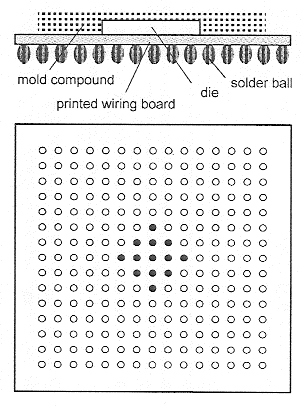
marked as solid were used for thermal vias and were connected directly to the ground layers of the mother board. The overall dimensions of the package were 27x27x2.13 mm. The test chip has the dimensions 12.7x12.7x0.4 mm. 2.3 Flotherm model of the PBGA225 Model Set-Up The Flotherm model was build up of three blocks: substrate, chip and molding. The thermal conductivities used are shown in Table 1. The bond wires as well as the chip bonding glue were neglected. The solder balls were set up of 225 rectangular cuboid elements. Their cross section was calculated to be the same as the cross section of the round shaped solder balls. The printed circuit board with its embedded copper layers was also build up of cuboid elements. The board thermal conductivity was set to 0.3 W/mK the thermal conductivity of the copper ground planes to 360 W/mK. The thermal vias in the printed circuit board were modeled as blocks embedded in the board directly underneath the central solder balls. Their dimensions were chosen to align exactly with the solder balls in order to simplify the computational grid. Symmetry along the vertical axis was assumed, therefore only a half of the package and of the printed circuit board were modeled. For the symmetry plane conditions of an adiabatic, impermeable and friction-less surface were set (external wall) [1]. The dimensions of the computational domain were set to align exactly with the printed circuit board dimensions. The computational domain extended 30 mm from both front and rear board surfaces. This proved to be sufficient to get the air velocity distribution along the component and board surfaces. The boundary conditions for a single board were applied, namely free stream boundaries for the top and side walls of the computational domain and the radiation exchange with the ambient. An external fan element was placed at the bottom of the computational domain to simulate the forced cooling. The emissivity of the component surface was set to = 0.9, the emissivity of the board surface to e = 0.8. The influence of the radiation will be discussed later.

Grid Dependence. Before the systematic simulation of the package was performed, the density of the computational grid inside the component and in air regions dose to the surfaces was varied to determine a sufficient nodalization. Sufficient means a grid which is insensitive to further refinement. Increasing the grid size leads generally to a decrease in the calculated temperatures- With progressive grid refinement the changes decrease until the computed temperatures do not depend on the grid size any more.
The chosen grid has typically 96063 cells, the computing time was about 180 mm on a Sparc Ultra l. Near to the component and board surfaces a non-uniform grid spacing was applied in order to ensure that the boundary layers were sufficiently resolved. Due to the large number of solder balls there was no need to add grid cells inside of the component in directions parallel to the board plane. However across the component thickness 5 additional cells were set. The contribution of radiation to the heat transfer depends on the thermal environment of the board under test- If the board is assembled in a sub-rack, the radiation exchange occurs between the board and its neighbors which have similar temperatures. In this case the contribution of radiation can be neglected. However, it a single board without thermal environment is tested - this is often done for thermal resistance measurements - the radiation exchange with the ambient cannot be neglected.
The contribution of the radiation exchange can simply be evaluated if the radiation in Flotherm model is deactivated and the temperature is recalculated. Deactivating the external radiation of the PBGA225 top surface only resulted in an increase of thermal resistance of 4%, deactivating both - component and board radiation - to an increase of 15%. The heat generated in the die can be represented in the software model either by a uniform heat dissipation of the whole chip or created in a thin layer underneath the chip surface. It was found that the calculated chip temperature was nearly the same in both cases. The reason is the high thermal conductivity of the silicon. The very small thermal resistance across the chip thickness ensures a uniform temperature distribution in the die, regardless of how the heat generation is represented. For the thermal resistance calculation the maximum chip temperature was used. Using the average chip temperature leads to a thermal resistance which is about 3% lower.
Table 1 - Thermal conductivities used for the PBGA225 model
2.4 Verification of the PBGA225 model The simulation model was run with different heat dissipations and air velocities. The calculated junction, package and board temperatures were then compared with the measured values. The results are summarized in Table 2 and Figures 3 and 4. The calculated junction temperatures correspond very closely to the measured values. The deviation of the junction-to-ambient thermal resistance is always less than 10 %. The calculated board excess temperatures are about 4 K lower than the measured values (Figure 3). The temperatures calculated for the component body differ by 12 K from the measured values. The deviations lie all within the measuring accuracy and show that chip temperatures as well as the board temperatures can be predicted with a very good reliability.
on boards with different ground planes (copper thickness 2x35祄 or 2x10⁵祄).
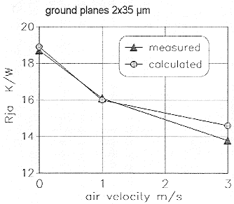 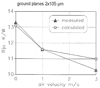
PBGA225 on boards with different copper ground planes 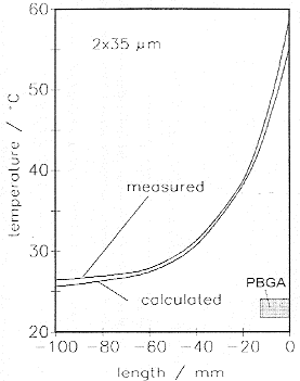 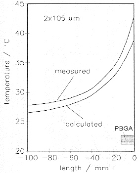
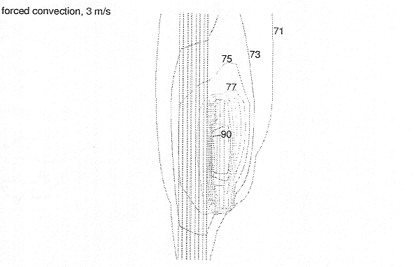
circuit board underneath the package center (natural cooling, PBGA225 with 3W, ambient 24C). The measurement was performed using an infrared imaging equipment. 3.1 Description of the SuperBGA352 model The experience gained by modeling the PBGA225 package was used for the thermal simulation of the SuperBGA352 (SBGA352) mounted on multilayer boards with different copper layer thicknesses. The purpose of this study was to evaluate heat dissipation limits for the package mounted on boards with different layer structure. The results were obtained using simulations only, no verification measurements were performed. The package is shown in Figure 5. The chip is bonded directly to the underside of a heat spreader. Most of the package body is composed of copper, which provides a high conductivity thermal path to the solder balls [2]. From here the heat can be conducted to copper planes in the motherboard. The Flotherm model of the package was build up of five blocks: copper heat spreader, copper ring, multi-layer, chip and molding with their appropriate dimensions and conductivities as shown in Table 3. The adhesive connections were modeled as two dimensional plates. The bond wires were neglected. The solder balls were setup of 352 rectangular cuboids in the same way as done for the PBGA225. The data used for the model were based partly on information from the component manufacturer and partly on an own analysis done in our qualification lab. Then the package was placed on three different boards, all with the dimensions 232x159 mm, and calculations were performed for different heat dissipations and different air speeds. The thermal environment in a sub-rack was considered (no radiation heat transfer and 70C ambient). The following boards were used:
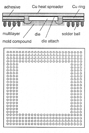
The chip had the dimensions 12.7x12.7x0.4 mm. The solder balls were connected only to the upper signal layer, no thermal vias were used.
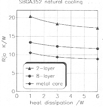
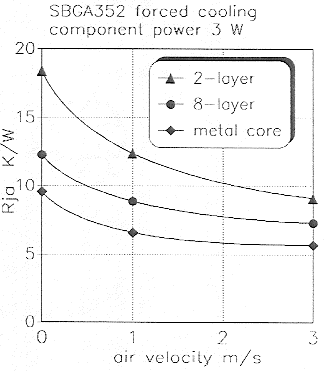
The printed circuit boards were set up of cuboid elements. Each copper plane was modeled separately. An effective thermal conductivity was calculated for each layer using the estimated copper share - in general 150 W/Km for a signal plane and 300 W/Km for a ground plane. The solder balls were connected only to the upper signal plane, there were no thermal vias to the ground planes. The calculated junction-to-ambient thermal resistances are shown in Figure 7. The wide range of the values (6 K/W to 20 K/W) shows that it is impossible to characterize the thermal performance of the package by a single value. The board structure and the environmental conditions have always to be taken into account. The importance of the board properties for the component cooling can be seen from the analysis of the heat fluxes done in Figure 8. Here the convective heat flux from the component surface is compared with the convective heat fluxes from different board regions. Depending on the board an amount between 6% and 17% of the heat dissipated in the component is delivered directly via the component surface to the ambient air The rest is conducted via the solder balls to the board and is then convected from the board surface to the ambient air Due to different lateral heat spreading capability of the boards the different board regions make a different contribution to this heat flow path.
This analysis shows the difficulty of predicting component temperature on a full populated board. The neighboring hot components cause an increase of the board temperature. The cooling capability of the board decreases and the component temperature is higher as calculated for a single component. The importance of this effect rises with increasing copper thickness in the board. In this case more detailed models are necessary which take into account the component thermal environment on the board. It was shown that using this CFD tool for a detailed thermal modeling of the components on multilayer boards leads to a very reliable results. The chip temperature as well as the temperature of the printed circuit board can be predicted with a good accuracy for a wide range of applications in telecommunication equipment. From these results the heat dissipation limits of a package can be evaluated taking into account the thermal environment of a specific application. By this way it is possible to optimize the thermal performance of an assembly without using cost intensive test boards. However, detailed modeling is only possible on condition of a detailed knowledge of the package build up and of the thermal conductivities of the materials used.
 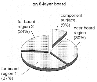 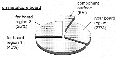
radiation not included). See Figure 9 for the definition of the board regions.
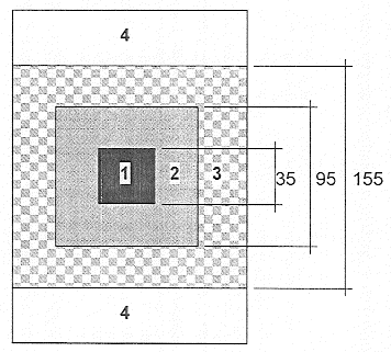
1 = Component Surface 2 = Near Board Region 3 = Far Board Region 1 4 = Far Board Region 2 Board dimensions 232x159mm. In the near board region, the rear side of the board directly underneath the component was included.
surrounding air (heat dissipation 3 watt, ambient temperature 70C) Acknowledgements The author would like to thank E. Schworm of Siemens AG for cooperation in selling up the PBGA Flotherm model.
The work was done as a part of the project "Simulation and Testing Methods" (SIMTEST) and was supported by the German Federal Ministry for Education, Science, Research and Technology (project 02PV12060). [1] J. Burgos, V. P Manno, K. Azar, "Achieving Accurate Thermal Characterization using a CFD Code - A Case Study of Plastic Packages', in IEEE Transactions on Components, Packaging and Manufacturing Technology, Pan 1, vol.18, No 4, 1995, pp. 732-738 [2] B. M. Guenin, R. C. Marrs, R.J. Molnar, 'Analysis of a Thermally Enhanced Ball Grid Array Package', in IEEE Transactions on Components, Packaging and Manufacturing Technology, Part 1, vol.18, No 4, 1995, pp.749-757 |
||||||||||||||||||||||||||||||||||||||||||||||||||||||||||||||||||||||||||||||||||||||||||||||||||||||||||||||

 沪公网安备 31010602003953号