


Plastic Quad Flat Pack
日期:2012-06-20
Development, Validation and
|
|||||||||||||||||||||||||||||||||||||||||||||||||||||||||||||||||||||||||||||||||||||||||||||||||||||||||||||||||||||||||||||||||||||||||||
|
H I Rosten and J D Parry, Flomerics Limited, 81 Bridge Road, Hampton Court, Surrey KT8 9HH, UK Abstract
A thermal model of a Plastic Quad Flat Pack (PQFP), developed using a computational fluid dynamics (CFD) program is presented. The model predictions are validated with junction-to-ambient thermal resistances measured in still air and infra-red measurements of the package and board surface temperatures. An application of a modified version of the model to a laptop computer is demonstrated. The work forms part of a long term programme to create and validate generic thermal models of a range of electronic parts. Background The motivation behind this work is to develop a standard thermal model of a PQFP which, once validated for a variety of PQFP designs, will serve as a generic thermal model for this package type. This model may then be applied to board and enclosure level predictions. The overall aim of the work is to show that such predictions can accurately be made and to encourage package vendors to provide numerical models of their packages. The inspiration for this approach was drawn from the following quote from Bar-Cohen, Elperin and Eliasi [1]
This approach was first demonstrated by Rosten and Viswanath [2] for a Ceramic Pin Grid Array (CPGA). The present work represents a logical extension to this. The work forms a part of a three-year European Union funded ESPRIT project named DELPHI which seeks to address the fact that the accurate prediction of junction temperatures at the component-, board- and system-level is seriously hampered by the lack of reliable standardized input data The electronic parts studied include a variety of chip packaging styles, beat sinks, fans, baffles and interfacing materials. A comprehensive account of this project is given by Rosten and Lasance [3]. The particular design of package studied in this paper is a 208-lead PQFP that was manufactured by members of JEDEC committee JC 15.1 for the purposes of evaluation of a new standard for the measurement of thermal resistance of SMT devices in still air conditions. Of course, the air is not still because the dissipated power initiates natural convection in the form of a thermal plume rising from the package: the phrase 'still air' is used to distinguish between measurements taken in an enclosure and measurements conducted in a wind tunnel with the fan switched off This new standard is intended to provide a sufficiently comprehensive statement of the procedure to be followed by an experimentalist so that different thermal test laboratories conducting measurements on the same part will reach the same results. To test this, a preliminary specification was written and test kits assembled which contained an environmental chamber, several samples of the 208-lead PQFP design mounted on a SEMI-style test coupon, a connector, a board support arid a thermocouple. The kits were circulated amongst committee members in a 'round robin' test. In consequence of the results reported several deficiencies in the original specification were highlighted, and the specification amended in the light of these experiences. At the time of writing (Jan 95), the final specification is being balloted by members. Background to this work is provided by Siegal [4]. Measurements of the junction-to-air thermal resistance and the surface temperature distribution were made for the device mounted on the test board specified by the proposed JEDEC standard. The device was mounted horizontally in the JEDEC enclosure, as specified, and vertically in a second enclosure as specified in the SEMI standard G38-87 for comparison. In each case the predicted and measured thermal resistances were compared. High spatial resolution radiation thermography was used to measure the temperature distribution on the top surface of the PQFP and the test board for comparison with the predictions.
In the following section, the details of the experimental procedures used are described, followed by a detailed description of the thermal model of the PQFP. Comparisons are then made between predicted and measured values of junction-to-ambient resistance. Excellent agreement is shown between the measured and predicted surface temperatures. The authors believe this may be the first such detailed comparison between CFD predictions and radiation thermography measurements at the package level. A brief discussion is then provided of the application of the model to a laptop computer with comparison between predictions and measured junction temperatures of packages on the mother board. In the conclusion attention is drawn to work done on the development of a "compact" thermal model of the PQFP. Experimental Procedure Experimental DetailsSurface temperature measurements and junction-to-ambient thermal resistances were taken from a 208-lead PQPP mounted onto a thermal test board. The device was supplied by the JEDEC JC15.1 committee. The committee produced the device in conjunction with a proposed new test methodology for thermal characterization of packages [11]. There are several standards, such as the SEMI [12] and MIL 13] ones, for the thermal characterization of IC component packages that have been in use for some years. However, it has been well documented that the results obtained from these methods are subject to considerable variance. Davies et al [14] concluded that thermal resistance varies with such factors as board orientation and copper content and distribution. Lin et al [15] showed that the thermal resistance can vary with such factors as power level, air flow and ambient temperature. Joiner [16] drew attention to problems with the SEMI method of determining junction-to-ambient thermal resistance. Further references on this subject are provided by Rosten and Lasance [3].
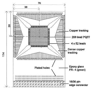
One of the aims of the JEDEC committee JC15.1 is to produce a specification for a method of thermal characterization which ensures repeatable results for thermal resistance for a specific package [11]. The package contains a test die consisting of a temperature sensitive diode and a sheet heating resistor covering 95% of the die surface, ensuring that the diode temperature is representative of the whole junction. The package is fully soldered onto a tracked epoxy glass FR-4 (green) test board shown in figure 1.
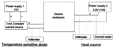
Measurement system Both JEDEC and SEMI test methods specified the use of the same equipment and connections for measuring the thermal resistance of the device. They differ in the specification of the enclosure and board orientation: the JC 15.1 specification focuses on a horizontal board orientation (but permits vertical boards as appropriate for high power devices); whereas the SEMI specification deals only with vertical boards. In the work reported here, the JEDEC board was mounted horizontally in the JEDEC enclosure and vertically in the SEMI enclosure. The thermal test device was powered by connecting a power supply to the heating resistor. A voltmeter and current meter were used to measure the power level. A 1 mA constant current source, powered by a second supply, was connected to the device to forward bias the diode which acts as the temperature sensor at the centre of the active surface of the die. The voltage across the diode was measured by connecting a voltmeter to the second power supply. The connections to the device are shown below in figure 2.
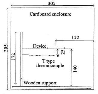
The JEDEC method stipulated the use of a square cardboard enclosure of side 305 mm. The device was mounted horizontally and held in place with a wooden stand. A T-type thermocouple was fixed in place under the centre of the package as shown in figure 3 (the final specification positions the sensor near the enclosure wall).
The SEMI specified enclosure consisted of a square box of side 305 mm with internal surfaces of low emissivity, to which end the box was constructed from Styrofoam internally lined with silvered foil.
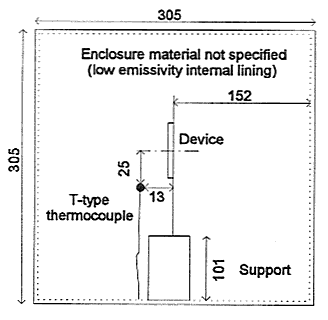
The device was mounted vertically and held in place by a Styrofoam support. A T-type thermocouple was placed in front of the package as shown in figure 4. The SEMI standards stipulate the use of a specific board for thermal characterization testing. During experimentation the JEDEC board was used, rather than the specified SEMI board, and tested according to the SEMI methods, enclosure and orientation. Before testing for junction-to-ambient thermal resistance, the temperature sensitive diode was calibrated in an environmental chamber to find the temperature sensitive parameter (TSP). The TSP is a relationship between diode voltage and junction temperature. The junction-to-ambient thermal resistance, denoted qja, of the package was found first using the JEDEC method and secondly using the SEMI standard. The package was placed into the JEDEC enclosure and powered up to 1W. The diode voltage and enclosure ambient temperature were recorded after thermal equilibrium had been reached. At least one hour was allowed for each test. qja was found by dividing the diode temperature rise by the power supplied to the resistor. An infra-red camera was then placed approximately 300 mm above the enclosure. The device was coated with black paint to ensure a uniform calibrated surface emissivity of 0.96. A section of the enclosure was removed and a picture of the surface temperature of the device in natural convection was recorded. The JEDEC device was then placed into the SEMI enclosure to measure the thermal resistance and surface temperature. In order to observe the effect of the internal lining the test for qja was repeated with the lining removed. A power level of 1 W was used for all tests. Thermal Model of the PQFP Thermal Analysis Software Used The detailed thermal model of this package was created using FLOTHERM? a commercially available CFD-based electronics cooling program from Flomerics [6]. An account of the mathematical foundations of this program is provided by Rosten and Viswanath [2]. The following sub-sections describe the way in which the constituent parts of the PQFP are modelled. Overview of the Thermal Model A picture of a typical PQFP is illustrated in figure 5 (the JC15.1 208-lead PQFP differs from this in that it does not have the comer 'bumps').
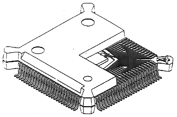
A picture of the FLOTHERM detailed model of the JC 15.1 208-lead PQFP is shown in figure 6.
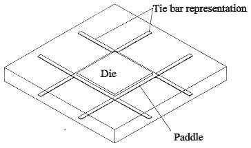
The structural items of the PQFP included in the FLOTHERM model are: the die, the die attach, the die paddle, the tie bars and the lead frame with all items encapsulated in a cuboidal volume of plastic mould compound. Important aspects of the modelling of these features is described below. Full details of the geometry and thermal properties of the package are provided in Appendix 1. The Plastic Encapsulant The plastic encapsulant was modelled as a solid cuboidal block of dimensions 28 x 28 x 3 mm. Of all parameters in the model, the most important is the thermal conductivity of the mould compound, because in a plastic package the mould compound represents the dominant thermal resistance. The value taken for this is 1.05 W/mK, a measured value provided by Edwards [5]. It is important to note that this value was assigned before the surface temperature measurements were taken, thus ensuring the validity of the comparisons drawn. The value given by Sumitomo, the manufacturer, was 0.62 W/mK, which is believed to be determined from the sum of the mould constituents rather than by direct measurement. It was important that the encapsulant was the first block entered in FLOTHERM because additional blocks needed for the representation of the interior structure of the package, for example the die, overwrite the properties of the previously entered blocks over the region in which they intersect. The order of entry of blocks is therefore critical. For full details of the rules see reference [6]. The Silicon Die and Power Dissipation The silicon die was modelled as a cuboidal block. The die was located with its lower surface positioned centrally on the top surface of the die paddle as can be seen in figure 9. The temperature variation of the thermal conductivity, k, of silicon is given by Blackburn and Hefner [7]. This is accounted for by using the following linearization of their formula:
an approximation which is accurate to within 3% over the operating range of temperatures. The JEDEC part contained a test die in which 1 Watt of power was dispersed across the upper surface of the die by a sheet resistor covering 95% of the upper surface. This power dissipation was modelled by a planar source of heat applied within the top surface of the die, covering 100% of the die surface. The Die Paddle The die paddle is treated as a cuboidal block of dimensions 11 x 11 x 0.1524 mm, the lower surface of which was set to be 1.1235 mm above the base of the package. The paddle, die and tie bars can be seen in figure 9. The paddle and lead frame are made from Cu-EFTEC 64T which has a thermal conductivity of 301.5 W/mK. The Die Attach The die attach is a very thin layer of adhesive material that glues the die to the die paddle. In FLOTHERM it is modelled as an internal plate which means that it has no thickness within the finite-volume grid, however, it does have a 'thermal thickness', which separates the adjoining grid cells. The thermal conductivity of the plate was set to be 2 5 W/mK, and its thickness was set to 0.05 mm. Hence the thermal resistance offered by this plate to the flow of heat from the die to the die pad is
which is insignificant. The reason the die attach was not treated as a cuboidal volume was because it would have caused a very thin layer of grid cells which can result in slow convergence of the iterative algorithm used to solve the equations for temperature. The transverse dimensions of the epoxy were set to correspond to those of the die.
A diagram of the lead frame is shown in figure 7 provided that the temperatures of the leads around the sides of the package do not differ too much between themselves, the heat flux lines will essentially take up a radial pattern. For heat flowing radially out along the lead frame the plastic and copper regions will appear as thermal resistances in parallel. For heat flowing vertically through the layer the plastic and copper will also appear as resistances in parallel. Parallel resistances are equivalent to conductivities in series, so the average thermal conductivity for the layer is given by:
where a represents the percentage of copper coverage. Bright [8] determined the coverage of 40% from the mechanical layout diagrams of the package giving an average conductivity of:
In the unlikely event that significantly different boundary conditions occurred at the sides of the package, the aforementioned practice would over-estimate the heat cross flow, because in cross flow the leads and mould are in series corresponding to a thermal conductivity heavily weighted towards the mould conductivity. A simple improvement is to account for this effect by using orthotropic conductivities.
In FLOTHERM the lead frame layer was represented by four cuboidal blocks of conductivity 121.2 W/mK as illustrated in figure 8.
As the heat source is situated at the centre of the package, The bond wires were neglected as they do not represent a significant thermal path due to their small cross-sectional area.
The tie bars protrude diagonally from the corners of the die paddle to the comers of the package. In the model each tie bar is represented by two cuboidal volumes that protrude out of the edges of the comer of the die paddle to the sides of the encapsulant, as illustrated in figure 9.
On each side of the package, the external leads are modelled by two solid cuboidal volumes having a thermal conductivity intermediate between that of air and copper using a weighting factor of 50%.
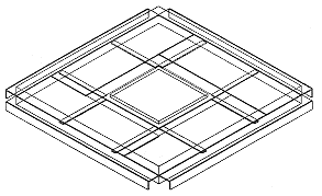
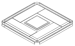
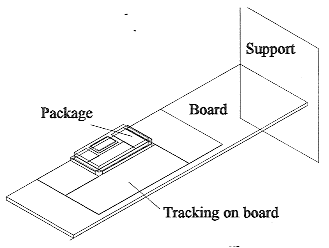
The test board to which the PQFP is attached is shown in figure 1. This includes allowance for the connector that attaches the board to the wooden support. The component, board and support are illustrated in figure 10 for the JC15.1 experimental arrangement. The epoxy board is made of FR-4 with a specified thermal conductivity of 0.4 W/mK. The copper trace on the board has a thickness of only 0.03556 mm, which is 2.25% of the board thickness. This was modelled by four cuboidal volumes of thickness 0.1524 mm, corresponding to 9.6% of the board thickness). The reasoning again was to avoid very narrow grid cells, the presence of which could hinder the iterative solution of the temperature equations.
a = thickness of the actual cooper trace The following formulae follow from application of the usual rules of: addition of conductivities for conduction paths in parallel, and addition of reciprocals for conduction paths in series:
It follows that:
the thermal conductivities being equal when the block thickness equals that of the trace. In the case of the board used for mounting the JC 15.1 208-PQFP for which the percentage coverage of the trace is 32%
the in-plane thermal conductivity of the trace volume is enhanced by the copper trace while the normal-to-plane conductivity is very close to that of the FR-4. In the model, the thermal conductivity of the copper-trace volume is set to the in-plane value of 30.23 W/mK. Since the copper-trace volume is only 9.6% of the board thickness, the contribution of the incorrect normal-to-plane value within the copper-trace volume to the total thermal resistance through the board is not significant. Again, this could be corrected by the use of orthotropic conductivities but it would make little difference to the results.
The thin air gap that separates the board from the package was modelled as a planar resistance to heat flow having a thermal conductivity of 0.0261 W/mK, and a thickness of 0.254mm. As in the representation of the die attach, the rationale for this being the avoidance of narrow grid cells.
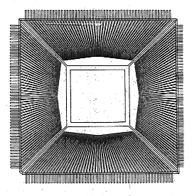
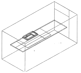
The enclosure used in the JC 15 specification is a square cardboard box of side 305 mm. However, the domain of integration was not extended to the boundaries of the enclosure. Instead the domain extended in to die air 25 mm below the board, 50 mm above the board, and some way to the side of the board. At the boundaries of the domain, free air conditions are applied, fixing the relative pressure to zero with any incoming air entering with the prescribed ambient temperature. Thus, we have not allowed for any bulk heating of the air within the enclosure as a whole which is a reasonable assumption for a device dissipating I Watt. In this connection, it is interesting to note that the final JEDEC specification includes an adjustment to account for the difference between the initial ambient temperature and the ambient temperature at the end of the experiment, measured in a plane 25 mm below the board but next to the enclosure side, it was demonstrated experimentally by Joiner [10] that locating it 25 mm below the centre of the board resulted in higher temperatures due to board proximity. By not extending the domain to the enclosure sides, the problems of specification of the thermal conductivity of the cardboard enclosure and the external heat transfer were avoided. A direct benefit is that the computational grid is used entirely to focus on the resolution of the boundary layers around the board and the package. The grid employed was 36x26x34 cells. The model is symmetric about a plane perpendicular to the board surface, therefore only one half of the problem is considered, significantly reducing the computational work needed to solve the air flow velocities, pressure and the temperature distribution within the air and the solid materials. The underlying physical assumption being made is that the thermal plume arising from the power-dissipating package is Symmetric about this plane. The extent of the solution domain with its boundaries is shown in figure 11.
The calculation takes a few hours on an 80486 PC.
Radiation sources with an emissivity of 1.0 were activated at the following surfaces: the board topside, the board underside, and the top surface of the package. The radiative exchange calculated was between each point on die solid surfaces and the enclosure at ambient temperature.
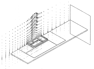
Figure 12 shows the predicted air flow pattern resulting from the power dissipated by die component in the JEDEC enclosure.
Evidently, the board acts as a heat sink, as 75% of the dissipated power enters the air via the board. Clearly, the still air measurement is in fact a characterization of the board-package assembly rather than the package alone. The draft JC15.l specification recognizes this fact in its preamble. At the time of writing the opening section of a draft JC 15.1 document entitled 'Environmental Conditions - Natural Convection (Still Air)' states: "The intent of the Rja, measurements is solely for a thermal performance comparison of one package to another in a standardized environment. This methodology is not meant to and will not predict a package's performance in an application-specific environment."
The point being that in a real environment the board will differ from the one used in the standard by virtue of copper content and adjacent powered components. Results of Junction-to-Ambient Resistance Measurements The power dissipation and enclosure ambient temperature boundary conditions in the CFD model were set to match those measured in the experimental tests. In both tests, a power level of I W was used. The ambient temperature in the JEDEC test was 21.5C and 21.3C for the SEMI test. The measured and predicted values of junction-to-ambient thermal resistance (C/W) are shown below in table 1.
thermal resistance values
The value of qja for the JEDEC board in the SEMI enclosure with the internal lining removed was 36.2C/W, so the internal finish of the enclosure appears to have little effect. This is confirmed by the following theoretical radiation analysis for an isothermal board within an isothermal enclosure: for the emissivity of the enclosure (eenc) to be immaterial, the following condition needs to be satisfied:
where a denotes the ratio of the surface area of the board to that of the enclosure, which is around 0.014. Re-arranging the above expression for the condition on eenc in terms of eboard (the board emissivity), we get:
Applying~=0.0l4 and eboard =1.0, we get the condition:
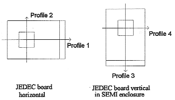
An almost imperceptible difference (probably well within experimental error) was seen between measurements taken in the SEMI enclosure with metal foil and with the metal foil removed. The surface temperature plots taken by the infra-red camera were compared with plots of the model produced by the CFD software. For illustrative purposes temperature profiles along the device centre lines were plotted for both sets of data. Centre lines were taken along the device length and width. Figure 13 shows the position of the profiles and the device orientation.
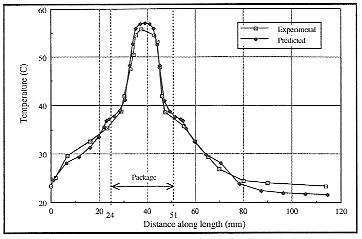
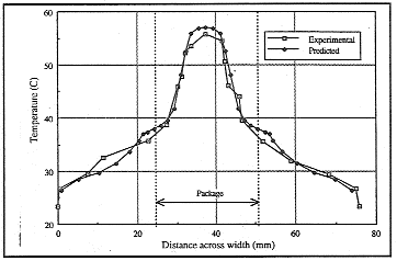
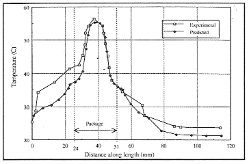
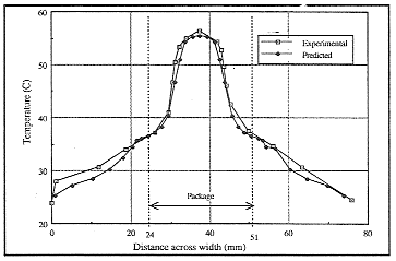
Discussion The junction-to-ambient thermal resistance figures compared very well. The predicted values were only 3.5% lower than experimental results for both the JEDEC and SEMI tests. This was within the range of experimental error and demonstrated that the computational model is able to predict the thermal resistance to within the range of the experimental error. The thermal resistance of the JEDEC test was higher than the SEMI test by 1.2 C/W. From this it was clear that board orientation had a much larger effect on the value of qja than the enclosure material or lining. Although the JC 15 hoard had a different copper distribution to that of the SEMI standard it had very similar dimensions. The SEMI standard specifies dimensions of 78 x 116 mm for the test board. Thus it was valid to use the JC15 board in a measurement otherwise done according the SEMI standard. Overall, the surface temperature profiles showed good comparison between experimental and predicted temperatures. In both profiles of the JEDEC test (figures 14 and 15) the comparison between prediction and experiment is good, being within the experimental accuracy of the radiation camera. 'Shoulders' appear in the predicted temperatures at the edges of the package which are less pronounced in the experimental results. This effect is thought to be due to the blocks representing the leads extending horizontally from the package until being vertically above the tip of the actual gull wing lead before bending to contact the board. The main discrepancy between prediction and experiment is seen in profile 3 for the SEMI test (figure 16) where the values for the package and board temperature were under-predicted, the maximum discrepancy being about 7C for the surface of the board vertically above the package, although this does not appear to affect the prediction of the junction-to-ambient thermal resistance for this configuration. it should be noted that the boundary conditions imposed in the computational model do not account for any stratification that may be occur in the experimental enclosure. However, this requires further investigation.
It is important to note that no modifications were made to the computational model to match these sets of data. The earlier sections have demonstrated the validity of the thermal model of the 208-lead PQFP for an isolated component in still air. In this section, an application of this model to thermal analysis at the system-level. The case considered is that of a laptop computer.
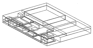
The PQFPs modelled differ from that described earlier in that they have an internal copper heat spreader attached to the bottom surface of the lead frame. The modification was achieved by extracting the standard model of the 208-lead PQFP from the FLOTHERM library of thermal models, adding a heat spreader, and replicating the resultant model six times in assembling a model of the laptop under consideration. The FLOTHERM model of the various components inside the laptop in the absence of the mother board is shown in figure 18. The keyboard is on the right located under which is the power supply and the disc drives. Figure 19 shows the mother board with three PQFPs visible on its top side, one directly visible on the bottom side of the PCB, and two partially obscured by the packages on the top surface.
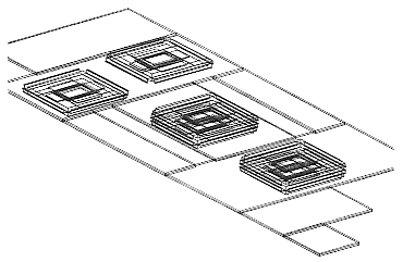
a PQFP package inside a portable computer
Concluding Remarks The pattern of work described by Rosten and Viswanath [2] in which a CFD model of a Ceramic Pin Grid Array package is first validated at the package level and then used in thermal analysis at the second- and third-level of packaging has been repeated for a 208-lead Plastic Quad Flat Pack. The thermal models of these specific components are accessible to FLOTHERM as library items. Limited numbers of these 'detailed' models of packages can be used in board- and enclosure-level thermal analysis. If
large numbers of such packages are present then very large models will result. The application to the laptop computer reported above is close to the limit of what is currently practical: the calculation took around 8 hours to run on an IBM RS6000/550 workstation. There is therefore a need to develop accurate simplified thermal models of packages. Such a 'compact' model has been developed for the JC15 208-lead PQFP as a part of the DELPHI project, [3]. A detailed account of this work is provided by Lasance et al [18]. Work is now in progress to construct a compact model of the CPGA package. Acknowledgment This work has been partially supported by the European Union under ESPRIT contract number 9197. References [1] A Bar-Cohen, T Elperin and R Eliasi, "Rjc characterization of chip packages - Justifications, limitations and future", IEEE Trans. Comp, Hybrids, Manuf. Technol., vol.12, pp. 724-731, Dec.1991 [2] H I Rosten and R Viswanath, "Thermal Modelling of the PentiumTM Processor Package", pp. 421-428, 44th Electronics Components and Technology Conference, May 1994, Washington, DC. [3] H I Rosten and C J M Lasance, "DELPHI: The Development of Libraries of Physical Models of Electronic Components for an Integrated Design Environment", in Current Issues in Electronic Modelling, Kluwer Academic Press, April 1995. [4] B S Siegal, "Thermal Characterization of Surface Mount Devices", pp. 99-107, Proc. 9th IEEE SEMI-THERM Symposium, 1993. [5] D Edwards, Texas Instruments, Private Communication, Nov 1993. [6] The FLOTHERM Reference Manual, pp. 4-37, FLOTHERM/RM/0394/1/1 [7] D L Blackburn and A R Hefner, "Thermal Component Models for Electro-Thermal Network Simulation", pp. 88-98, Proc. 9th IEEE SEMI-THERM Symposium, 1993. [8] B Bright, NCR, Private Communication, Aug 1993. [9] P Holshuijsen, Philips CFT memorandum, 22 Nov 1994. [10] B Joiner, memorandum presented to JC 15.1 committee, Atlanta, Sept 1994. [11] JEDEC committee, JCl5.1 Thermal measurement round robin procedure, (1992) B. Siegal, OAI. [12] SEMI International Standards, (1992), G38-87 Test Method for Still and Forced Air, Junction to Ambient Thermal Resistance of Integrated Circuit Packages. [13] US Military Standards, (1983), MIL STD 883C, Method 1012.1, Thermal Characteristics. [14] M Davies, J Lohan, I Punch and T Moore, "The Thermal Characteristics of a Board Mounted 160 Lead Plastic Quad Flat Pack", Proceedings of the EUROTHERM Seminar 29, 993. [15] PC Lin and L I Nquyen, "Thermal Characteristics of IC Packages", Proceedings of the EUROTHERM Seminar 29, 1993. [16] B Joiner, "Evaluation of Thermal Characterization Techniques", Presented at IEPS Conference, 1994. [17] R Viswanath arid I Ali, "Thermal Performance of High Performance Packages in Portable Computers", Proceedings of the 45th Electronic Components and Technology Conference, Las Vegas, NV, May 1995.
[18] C J M Lasance, H I Rosten, H Vinke and K-L Weiner, "A Novel Approach for the Thermal Characterization of Electronic Parts", Proc. 11th IEEE SEMI-THERM Symp., San Jose, Feb 1995. APPENDIX 1: Details of the PQFP Model
Table 3: Geometric data for JEDEC 208-PQFP
Table 4: Physical property data for JEDEC 208-PQFP |
|||||||||||||||||||||||||||||||||||||||||||||||||||||||||||||||||||||||||||||||||||||||||||||||||||||||||||||||||||||||||||||||||||||||||||

 沪公网安备 31010602003953号