


使用FLO/EMC建模设计回馈换流器
日期:2012-06-19
Flyback Converter Modeling Design Using FLO/EMC |
||||||||||||||||||||||
|
Author: John Maggs LO/EMC was recently employed in the modeling of a flyback converter at the PCB level. The model created was particularly unusual, as the model developed had to take into account the tracks on the PCB, as these were the area of the model that was going to be excited to generate the radiated emissions profile.
Model Details
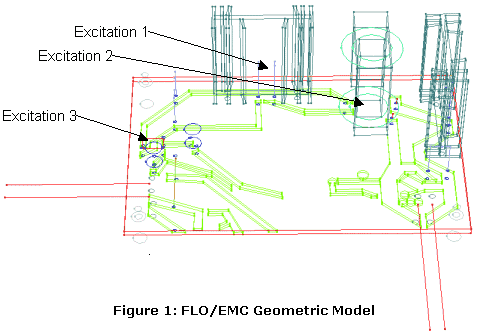
The PCB itself was relatively small (120 x 50 x 80 mm in total), and contained tracks on only one side. As far as the model was concerned only the areas which were going to be excited were modeled, as a problem with modeling large numbers of PCB tracks is that the models cell count can increase drastically due to the small cells used to model the tracks and correspondingly the time step can become very small, hence the simulations take a long time to run. Also due to the fact that flyback converter was not going to be modeled within any form of enclosure, these additional tracks could be assumed to have minimal effect on the radiated emissions profile over the frequency range of interest (30 - 1000 MHz). Also the PCB dielectric was not modeled as it was assumed that to be transparent to the electromagnetic energy at the frequencies of interest, the physical size of the PCB is present in the geometric model for the purpose of locating the tracks / components in the correct positions only. Compact cable models were used to simulate the power input and power output sides of the PCB as long cables can be a significant source of emissions, both radiated and conducted. The metal work of the two heatsinks located on the top side of the PCB were simulated as previous work done by Flomerics has identified that heatsinks, like cables, can be a significant source of radiated emissions. A diagram showing the geometric model created in FLO/EMC is shown in Figure 1 below.
As shown in Figure 1 the model was excited at three points, and the detail of these excitations are defined in Table 1. Table 1: Model Excitations
The details if the simulation is specified in Table 2.
Table 2: Simulation Details
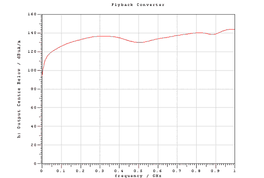
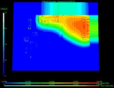
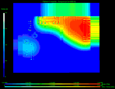
Model ResultsThe results obtained from the model were all at a point 12 mm below the PCB (in line with the manufacturers measurement techniques), and the electric and magnetic fields obtained at this point in the center of the PCB are shown in Figures 2 and 3 below. Note the results could not be compared to the limits for this type of equipment, as the monitoring point was located in the near field. Figures 4, 5 and 6 show the level of electric fields produced at a point 12 mm below the PCB at 30, 100 and 200 MHz respectively to identify the area of the PCB which is producing the emissions. 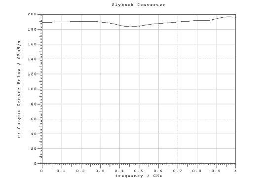 Figure 2: Electric Field 12 mm Below PCB
Figure 3: Magnetic Field 12 mm Below PCB
Figure 4: Electric Field Profile at 30 MHz, 12 mm above Board
Figure 5: Electric Field Profile at 100 MHz, 12 mm above Board
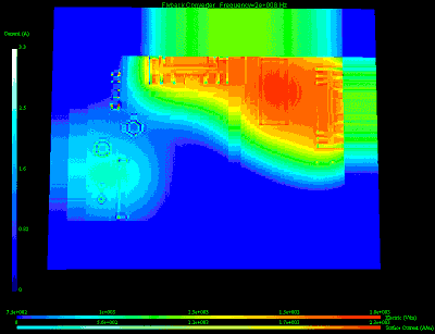
Figure 6: Electric Field Profile at 200 MHz, 12 mm above Board
Looking at the electric field profiles shown in Figures 4, 5 and 6 it can be seen that the majority of the field produced by the power supply is concentrated in the top right hand corner of the PCB where the transformer is located. The measured results showed a similar trend in terms of both levels achieved and the location of the maximum fields produced.
Conclusions
The model and results shown in this case study demonstrate the capability of FLO/EMC to be used in the simulation of PCB's and component level systems to determine any potential EMC problems that may exist. |

 沪公网安备 31010602003953号